In-sensor computing as a new paradigm for smart sensorics- ATOSENS
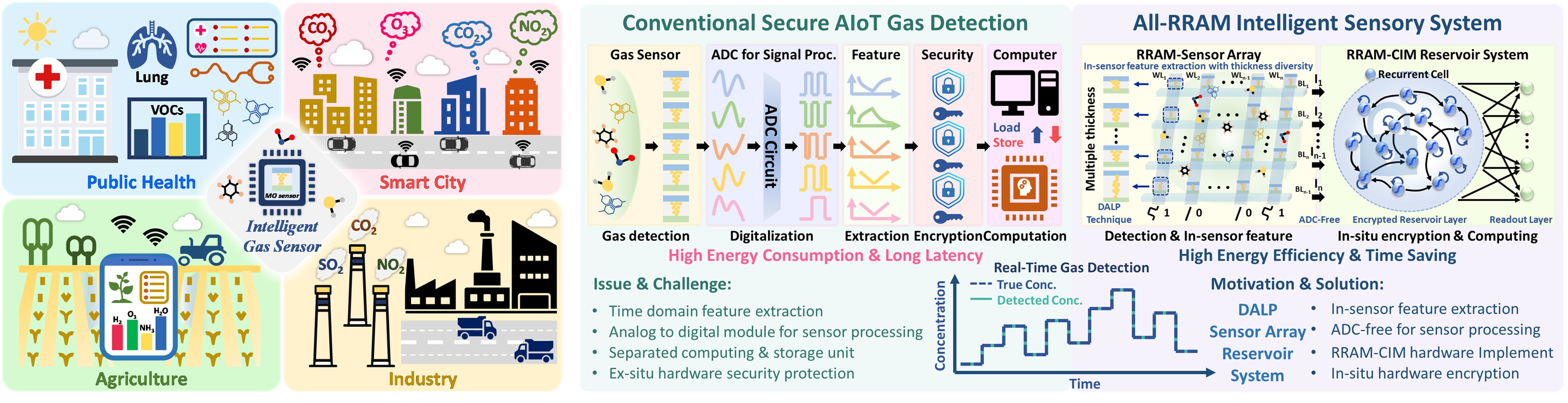
The M-ERA.NET ATOSENS project aims for an advanced intelligent gas sensing concept based on an in-sensor computing architecture, addressing key limitations of conventional gas sensing systems, such as high-power consumption, reliance on external data processing, and limited real-time capability. In this project, the researchers adopted a novel thin film fabrication technique – direct atomic layer processing (DALP) – enabling localized, atomic layer deposition of TiO₂ films for H2 sensors. This additive nanofabrication approach enables lithography-free, scalable fabrication of sensor arrays with precisely engineered material properties, while significantly simplifying the overall process flow. The resulting vertical TiO₂-based RRAM sensors exhibit high sensitivity to hydrogen, combined with rectifying diode behaviour that enables dense, transistor-free array integration. A distinctive feature of the developed system is the exploitation of thickness-dependent sensing characteristics to generate diverse, physics-based features directly within the sensor array. These features are processed in-situ using an RRAM-based in-memory computing platform implementing reservoir computing, allowing real-time gas concentration detection with high accuracy while minimizing data movement and latency. By eliminating the need for analog-to-digital converters and external feature extraction, the system significantly reduces hardware complexity, energy consumption, and system footprint, making it highly suitable for edge deployment. Furthermore, the approach leverages intrinsic device-to-device variability in RRAM elements to implement hardware-level security, enabling unique and physically unclonable system behaviour without additional encryption overhead. This combination of sensing, computation, and security within a single platform represents a significant step towards fully autonomous intelligent sensing systems. Overall, the project demonstrates a compact, scalable, and energy-efficient solution with strong potential for applications in hydrogen safety, environmental monitoring, and next-generation edge AI systems, contributing to the advancement of functional materials and integrated electronic devices. The scientific excellence of this work has been recognized by its acceptance for presentation at the highly selective IEEE International Electron Devices Meeting (IEDM) 2025 held in San Francisco in December 2025. The consortium has leveraged the complementary expertise of its members, namely: Institute of Electrical Engineering of Slovak Academy of Sciences, Bratislava, Slovakia – responsible for sensing device vehicle cleanroom fabrication and electrical characterization, and project coordination, Commenius University Bratislava, Slovakia, for gas sensing characterization, National Yang Ming Chiao Tung University, Hsinchu, Taiwan, for electronics design, compute-in-memory reservoir platform and neural network algorithm design, and Atlant 3D Nanosystems, Taastrup, Denmark, for implementing their proprietary Direct Atomic Layer Processing technology for target thickness deposition of TiO2 sensing layers. The IEDM 2025 paper can be found at IEEExplore, as T. -L. Chiang et al., "Direct Atomic Layer Processing TiO2 RRAM Gas Sensor for Real-time All-RRAM Intelligent Gas Perception," 2025 IEEE IEDM,doi:10.1109/IEDM50572.2025.11353891